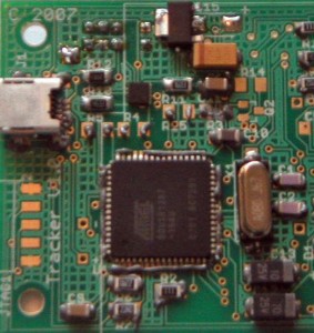
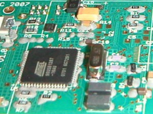
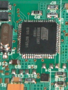
Having worked in the electronics industry for 30+ years I have had my fair share of problems making the change to surface mount technology (SMT). As a hobbyist I thought of SMT soldering as a new source of hair loss. Yet the lack of plated through hole (PTH) components has finally pushed me to embrace this technology for my hobby interests. My only regret is that I didn’t do it sooner. To my surprise I can actually assemble surface mount boards faster and with fewer problems than the old plate through hole designs that I had clung to. Furthermore, I have not had to invest in any complex or expensive equipment; most of the tools are available from around the house. I would like to share my discoveries with the rest of you so that you to can benefit from this simple change to SMT.
Assembling surface mount boards requires a few new tools; starting with a good pair of tweezers, a magnifying glass, a syringe of solder paste, solder wick and a re-cycled toaster oven. The procedure I use is simple and yet it allows me to design single and double-sided surface mount printed circuit boards (PCBs) using the latest in chip technology. I generally stick to 0805 capacitors and resistors because they are slightly easier to handle than 0603 devices. The finer the device the less coffee you can drink because a jittery hand is not very helpful.
The basic procedure is as follows:
Step 1 Solder Paste

Apply solder paste from the 20guage needle tip on the solder syringe, to the PCB pads.
For SMT resistors and capacitors a pin head drop of solder is all that is required.
For SMT ICs I run a bead of solder paste across all of the pins. Yes this looks like it will short everything out but physics will help fix this.
Alignment of TQFP and 0.8 mm pitch or finer components requires a bit more effort ……See special procedures.
Step 2 Reflow
200C for 4 minutes – This bakes out the humidity trapped in the package and avoids having the devices fracture under steam pressure. Pop-corning.
350C for 2 minutes – This is the pre-dwell time to liquefy the solder flux and bring the board close to the re-flow temperature without overheating everything.
500C for ~20seconds – This is the re-flow stage and the timing depends on the thermal mass of your toaster oven. The idea is to carefully watch for the solder to flow and once it has you turn off the oven and open the door to assist in rapid cooling. These temperatures could damage your parts if you leave things to long but I have not yet had any problems.
Before the solder solidifies gently tap the toaster oven to help align the components. Capillary action of the wetted solder helps to pull the components into alignment over the solder pads and the meniscus of wet solder helps to isolate what had been previously shorted pins.

Step 3 Tidy with solder wick
After re-flow, solder shorts are removed with a regular fine tipped soldering iron and solder wick. Use the magnifying glass to determine if there are any shorts between pins. Correct as required with solder wick. That is, apply the solder wick across the shorted pins and heat with a soldering iron until the solder melts and flows into the solder wick.

Special procedures:
Plastics: Plastic components like headers, battery holders and switches that are not normally re-flowed or are considered PTH devices should be manually soldered after re-flowing the board. This is done because the plastics in these devices tend to flow or deform at the higher re-flow temperature. If in doubt, test the component at 500C in the toaster oven to see if it melts or deforms.
Leadless chips: Devices with no exposed pins like the CASON8,DFN10, QFN etc. are best prepared by first applying solder to the pads using a quick re-flow (no pre-heating is required since you are only re-flowing solder on the bare PCB). After cooling the PCB is assembled as above and finally these small devices are aligned to the pads before re-flow. This procedure ensures that the amount of solder on the pads does not allow solder bridges to form underneath the components where they would not be detected and where solder wick is ineffective. Use solder flux to help seat the device during the final re-flow. It helps if the pad geometry is extended outside the package limit as this allows you to run a solder iron around the periphery of the chip if there are any opens or shorts.
TQFP: TQFP devices are first tack soldered to the board with two pins located on diagonal corners. First wet the pads with solder then manually place the TQFP aligning it over the pads. Re-flow one corner with your soldering iron (no extra solder is required). Now check the alignment with the magnifying glass and if things are lined up solder the second diagonal corner down. If things don’t line up you can re-flow the one soldered pin and move the device into position. Re-check the alignment with both corners soldered down. Now you proceed as above by running a bead of solder paste over all of the pins. Continue with the remaining SMT parts and then re-flow the whole board. This procedure is required because the lead spacing of the devices is so tight that the pins might not be well aligned to the pad resulting in solder bridges and shorts. Without this step the fine 0.5mm pins can sit in the gap between solder pads and turn the whole thing into a short circuit. When this happens capillary action cannot overcome the problem as the pins are physically stuck in the trough between pads.
Double Sided SMT: To make double sided boards you first assemble the least populated side of the board and re-flow the assembly. Next you assemble the top side of the board and re-flow that. Note that capillary action keeps the upside down components from falling off the board. Also the secondary side never gets as hot as the primary side during the brief re-flow period so the devices remain in place.
PartsList:
- Solder paste Digikey part #KE1507-ND $52.13
20AWG needle tip
tweezers
solder wick
magnifying glass
40W soldering iron with a fine tip
toaster oven (for exclusive use as a re-flow oven