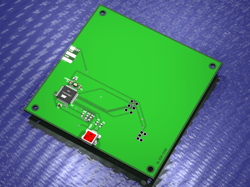
The last discussion about pogo pins was my first excursion into there use. The result was a purpose built programmer board to burn the capacitive touch switch firmware. I am less than thrilled with the complexity of assembling a test jig using these pogo pins. In response I have decided to try a new approach using Mill Max spring loaded pins directly soldered to a PCB (Digi-key part # ED5065-ND). The new solution consists of a custom PCB programmer which has a set of spring loaded pins soldered into it. The primary side only exposes the pins while the secondary caries all of the circuitry. The alignment of PCBs to the programmer is accomplished using laser cut templates. The Mill Max pins are larger in diameter than the previous pogo pins. In fact they are so large that I may not be able to place them in 0.1″ centers. This would require me to re-spin the capacitive sense board .
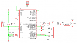
The programmer uses a low cost ATMega32U4 set up as a MKII TPI programmer just like in the previous post. I used Flip to program the on-board programmer for the first time. The schematic requires only a single device and it would be very easy to use an Arduino Leonardo for the hardware. The three pads on the edge of the PCB allow the boot loader to be engaged by dragging a dime over it. This is used to enable re-programming of the programmer.
The new through hole PCB spring pins are soldered into the primary side of the PCB. This eliminates all of the hand wiring required in the last prototype and I think this will be more reliable. The spring pins also have a shorter plunger action so that the board being programmed will sit flat when being programmed. To align the target boards to the contacts I have laser cut a template that has a hole that is just large enough to capture the target board. The target PCB outline is used as a reference to align the programmer to the contacts. You simply press the target board into the laser cut recess in the template and hold it in place while the board is programmed. Once programmed you just turn the whole assembly over and the board drops out.
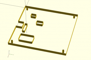
To secure the safety of the PCB programmer I have added a laser cut package to the back side of the PCB. This allows you to place the programmer on a table without worrying about shorts or damaging the secondary side components. The laser cut acrylic creates window holes where the components are, in effect recessing the chips 1/4″ into the plastic.
To create the backside template I print the Eagle board files to a PDF file which I can import into Inkscape. The board file becomes a template for drawing on after I scale it so that the PCB outline and Inkscape dimensions match. I drew rounded corner boxes around all of the secondary side components so that when they are laser cut in acrylic there will be no material to contact the chips. I then convert the drawing to pathes and flatten the curves to lines which allows me to export the design as a DXF file. The DXF file allows me to import the design into OpenSCAD so that I can review it as a 3D model.
Exporting to DXF
1. Set the stroke to 0.001″
2. Convert all objects from “stroke to path”
3. Under “Extensions->Modify Path->Flatten Bezzier”
4. Export to DXF as an LWPolyline
Rules
Don’t allow objects to touch one another. If they intersect you need to combine them into a single path.
Note that with Inkscape the XY coordinate shows the position of the lower left hand corner of the object.


